Are These Bad Solder Joints?

Joined
Mar 12, 2014
Messages
546
Reaction score
12
Location
Kansas
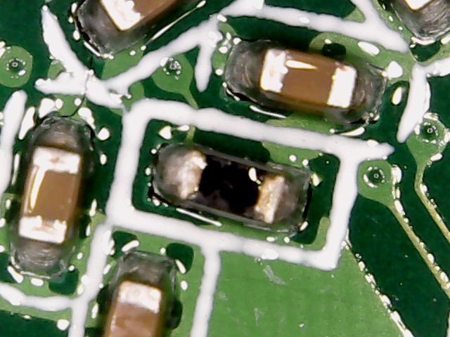
The pic shows some typical solder joints on my PV2+ onboard WIFI card. I suspect that the board has overheated which is apparently a common problem that drops the video to the mobile device. I get video feedback for about 60 seconds when the bird is powered up cold a
WIFI_1.jpg
nd then it drops the video but still shows telemetry on the app.
I notice that all the solder joints are a dull color as shown in the pic and wondering if that indicates bad connections. Shouldn't the solder be bright?
Also wondering where I can find the circuit diagram of this WM301_WIFI_2G_V1 circuit card that is one of the two cards in the wifi module. Is it possible to repair the board by reflowing the solder using a home oven?
 
I wish the image was a bit clearer.
Do you see any cracks in the solder?
Color usually is a reflection of the temp on the original solder joint.
Doesn't always mean it is a bad joint or connection. Hairline cracks at the edges of the joints is pretty much a dead give away from my experience, usually caused by vibration of a cold joint.
 
Here's another area of the board that shows what may appear to be cracks in a solder joint. I'm trying to avoid spending $200 on a new WIFI module so probably don't have much to lose in trying to reflow the solder. There are lots of youtube videos on reflowing solder.
I would like to find the website where circuit board numbers can be searched. I believe it's from when the circuit board design is submitted for approval but can't remember the name of the electronics association that does the approvals.
WIFI_2.jpg
 
Well, you could try to re-flow the solder to shore up the cracks.
If it don't work, you are still looking at replacing the board I think.
But....if it works, easy fix.
 
Can't see it with naked eye and the pic is shown with about 50X magnification. Maybe a piece of lint?

Looks like it was embedded in the solder paste before flowing.
 
Pics of the front and back of the WIFI board. Kinda blurry but wondering if anyone can identify the main wifi chip?
board_1.jpg
board_2.jpg
 
Can't see it with naked eye and the pic is shown with about 50X magnification. Maybe a piece of lint?

Looks like it was embedded in the solder paste before flowing.

Lint would not survive reflow.

Dull appearance is one indicator of lead-free solder.
 
  • Like
Reactions: Fplvert

Recent Posts

Members online

No members online now.

Forum statistics

Threads
143,090
Messages
1,467,571
Members
104,974
Latest member
shimuafeni fredrik